The growing demand for data-intensive artificial intelligence (AI) applications has highlighted the need for advanced memory devices that can keep pace with computational requirements. Traditional flash memories, while widely used for their non-volatile storage capabilities, often fall short in speed and efficiency for AI operations. Recent innovations in memory technology have focused on leveraging two-dimensional (2D) materials to create faster and more efficient flash memories.
Researchers at Fudan University have made significant strides in this area with their new approach for integrating ultrafast 2D flash memory devices. Their work, published in Nature Electronics, addresses the challenges of scaling and integrating these high-performance devices, which had previously hindered large-scale commercialization.
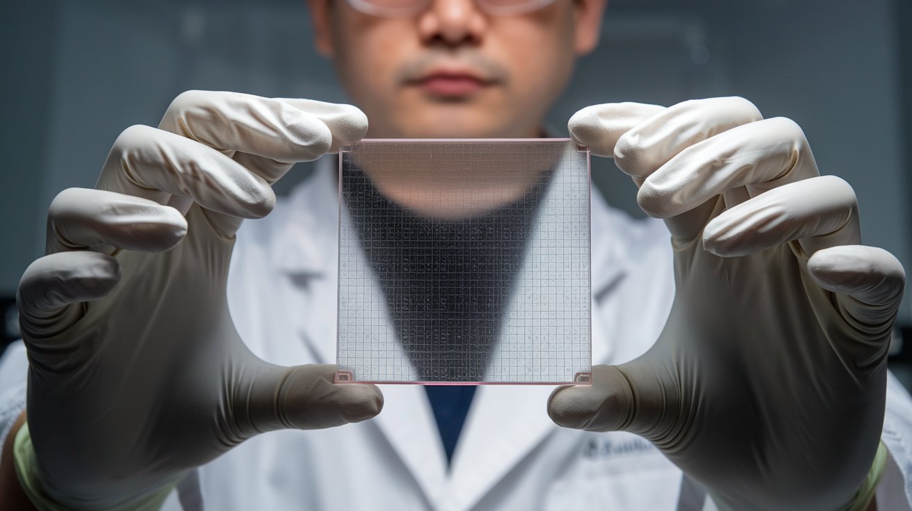
The research team, led by Yongbo Jiang and Chunsen Liu, reported a scalable integration process that successfully combined 1,024 ultrafast flash-memory devices with a yield of over 98%. This achievement marks a significant advance in the potential of 2D materials for memory applications.
“Two-dimensional (2D) materials could potentially be used to create ultrafast flash memory,” the researchers noted in their paper. “However, due to interface engineering problems, ultrafast non-volatile performance is presently restricted to exfoliated 2D materials. We report a scalable integration process for ultrafast 2D flash memory that can be used to integrate 1,024 flash-memory devices with a yield of over 98%.”
The team's approach involved a combination of advanced processing techniques, including lithography, e-beam evaporation, thermal atomic layer deposition, polystyrene-assisted transfer, and annealing. This methodology enabled the fabrication of memories with two different tunneling barrier configurations (HfO2/Pt/HfO2 and Al2O3/Pt/Al2O3) using monolayer molybdenum disulfide, a type of 2D material.
One of the key innovations was the ability to scale the channel length of the flash memories down to sub-10 nm, surpassing the physical limits of traditional silicon flash memory. The sub-10 nm devices demonstrated ultrafast speeds, non-volatile information storage (up to 4 bits), and robust endurance (over 10^5 cycles).
“Our sub-10 nm devices offer non-volatile information storage and maintain robust endurance,” the researchers stated. “This represents a significant advancement in the capabilities of flash memory technologies.”
The successful integration of these ultrafast flash memories with high yields suggests a promising future for their deployment in various high-performance computing applications. Future studies will likely explore additional 2D materials and memory stack configurations, further enhancing the potential for large-scale adoption of these advanced memory devices.
As AI and other data-intensive technologies continue to evolve, the development of faster and more efficient memory solutions will be crucial. The advancements made by the Fudan University team represent a significant step towards meeting the growing demands for high-bandwidth memory solutions in modern computing.